Placement at Edwards Vacuum: my experience in the semiconductor industry
Interested in the semiconductor industry or want to know more? Have a read of this excellent blog by one of our placement students!
My name is Samad Anjum and I am an undergraduate student at the University of Bath, studying Natural Sciences. I am currently in placement-year, working at a company called Edwards Vacuum.
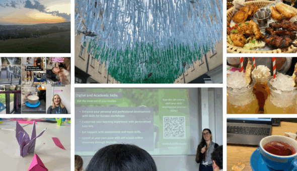
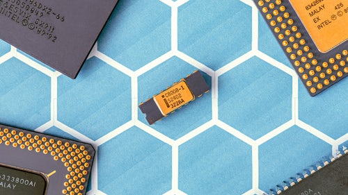
A big name in the semiconductor industry, Edwards Vacuum develops and manufactures tools for advanced processes, such as semiconductor, flat panel display and solar cell manufacturing. As implied by the name of the company, these tools certainly include vacuum pumps, but the company also develops exhaust management systems, which is the division in which I work. I am enjoying a wealth of experiences and opportunities at Edwards, including a visit to a semiconductor fabrication plant (including tour of the cleanroom, in a “bunny-suit”!) and representing Edwards at the Big Bang Science Fair and SEMI Talent Forum at the University of Bristol!
This post answers some of the questions about my experiences on placement, what hopefully is the start of a great career in the semiconductor industry.
To find out more about semiconductor careers, come and visit the SEMI Talent Forum, a two-day careers event hosted at the University of Bristol on the 2nd and 3rd May 2019. The event aims to bring together students, the GW4 universities (Bristol, Bath, Exeter & Cardiff), companies and government agencies, and is an excellent opportunity for networking and forming industrial contacts. There will be lots of seminars and full-day workshops with opportunities for interview preparation, mentorship and tech shows! I will be answering your questions at the Edwards Vacuum booth and demoing our virtual reality video game, so come and say hi!
What is your role?
My role is in R&D of exhaust management technologies for Edwards gas abatement systems used in advanced manufacturing processes, most importantly semiconductor manufacturing. These are fuel-powered incinerator systems which purify exhaust emissions from manufacturing facilities, by chemically reacting or decomposing greenhouse gases and chemical species which are toxic, unstable/explosive or otherwise harmful to health or the environment, so that only clean air is released into the atmosphere. These systems play an especially important role in the prevention of anthropogenic climate change.
The technology team of a dozen colleagues and I are developing a variety of innovative technologies, with the aims of maximising the destruction of dangerous/harmful gases without producing nasty by-products, increasing system uptime, and consuming as little fuel/energy as possible. These are experimental technologies in their early stages; however, promising technologies can be further developed and potentially incorporated into future products.
Why did you apply for this placement?
As Edwards Vacuum are a major supplier of tools to semiconductor companies like Intel, Samsung and Micron, I saw a placement there as a great opportunity to kick-start a career in the semiconductor industry and gain invaluable work experience which is highly sort after by companies.
And as for why I am interested in the semiconductor industry: semiconductor devices are short-lived, the market is volatile, and rapid technological advancements are required to drive the $500 billion industry to growth [1]. Our smartphones, computers and consumer technologies can only evolve as much as the semiconductor devices powering them, so there is a strong and constant demand from the consumer level for technological advancements in the industry. It is fast paced, highly innovative, and constantly and rapidly evolving - there really is no other industry like it.
What do you do on a day-to-day basis?
I work in a gas laboratory, using my experimental gas abatement system to destroy mixtures of known concentrations of gases as effectively as possible. I use analytical techniques such as infra-red spectroscopy to analyse exhaust emissions and characterise system performance under various reaction conditions and setups. I independently design my experiments, modifying my abatement system as required, occasionally producing CAD models/technical drawings where necessary and building required parts in a machine workshop. I use scientific programming languages to analyse the results of my experiments, the outcomes of which I use to design further experiments. I also present these findings to my colleagues at monthly discussions.
Alongside these day-to-day duties, I am currently preparing to represent Edwards Vacuum at the Big Bang Science Fair in Weston-Super-Mare next month, where I hope to introduce and inspire many young minds into the amazing world of STEM! I am also planning the same for the older minds too, at the SEMI Talent Forum at the University of Bristol. More on that later…
I basically blow things up!
What are your future plans?
After graduation, I would like to pursue a postgraduate degree qualification in a subject along the lines of semiconductor engineering, before working in the industry. I want to develop technologies for the processing of more complex semiconductor devices, to enable innovation in electronics, particularly in the fields of AI, autonomous vehicles and graphics rendering. In terms of career, I am certain that I want a bit of academia and a bit of industry.
Why do you think other students should consider this industry? What advice do you have for students interested in this field?
STEM students - the semiconductor industry needs you! If you aren’t yet sure about what career path you’d like to take, consider the semiconductor industry. Semiconductor processing is complex and incorporates many disciplines across the physical sciences and engineering subjects. This fast-paced, highly innovative and rapidly evolving industry needs bright minds in order to flourish. You can see that the work that I am doing at Edwards Vacuum is heavily based on physics and physical chemistry, but this is like a drop in the ocean compared to the range of work that is available in the industry. From the development of process tools, to research into technologies to increase transistor density, and even environmental management, there is something in the semiconductor industry for every STEM subject. You can rest assured that your work in the industry will make a huge difference to the world, as advancements in semiconductor processing technologies directly lead to innovation in electronics. This means, amongst many things, cooler iPhones!
What advice do you have for students going on placement next year?
Placement opens up a whole world of opportunity for career and personal development – it’s life-changing, so if you get the chance to apply for placement as part of your degree programme, go for it! Employers regard the experience highly – the way my supervisor explained it to me, he views a 12-month placement as at least 2 final-year projects, so a student with a bachelor’s degree with placement is more appealing to companies than a student with an Integrated Master’s degree without placement.
Working in a new environment may seem daunting at first but you will find that you eventually settle in quite quickly and adapt to the new lifestyle. On your first few days of placement, ask lots of questions and remember to take down notes, as you may be told a lot more than you can remember. Also, know what you are capable of doing and what skills you would like to develop, and discuss these with your manager/supervisor – this is to ensure that you never find yourself with too little or too much to do. Try to tailor your projects so that you can develop the skills you would like to work on. I personally wanted to improve my programming skills on placement, so I started using Python for my data processing and I’ve learned so much from that.
While you are on placement, you have the greatest opportunity of your entire undergraduate life to network and gain recognition in industry, so accept all the opportunities you can to travel and form contacts in the industry, organise events and attend tours. In terms of development, these opportunities are probably worth much more than your projects!
Final words
Placement year could be one of the greatest years of your life, and potentially the start of your career. By going on placement, you are opening yourself up to development and future career opportunities including job offers! Be productive, learn a lot and just enjoy the whole experience! Who knows where it’ll lead you?
To find out more about semiconductor careers, come and visit the SEMI Talent Forum, a two-day careers event hosted at the University of Bristol on the 2nd and 3rd May 2019. The event aims to bring together students, the GW4 universities (Bristol, Bath, Exeter & Cardiff), companies and government agencies, and is an excellent opportunity for networking and forming industrial contacts. There will be lots of seminars and full-day workshops with opportunities for interview preparation, mentorship and tech shows! I will be answering your questions at the Edwards Vacuum booth and demoing our virtual reality video game, so come and say hi!
[1] https://www.semiconductors.org/global-semiconductor-sales-increase-13-7-percent-to-468-8-billion-in-2018/
Respond